

| Place of Origin: | China |
|---|---|
| Brand Name: | SCANMAX |
| Certification: | CE,CF,RoHS |
| Model Number: | FT10 |
| Minimum Order Quantity: | Negotiable |
| Price: | Negotiable |
| Payment Terms: | L/C, D/A, D/P, T/T, Western Union, MoneyGram, Paypal |
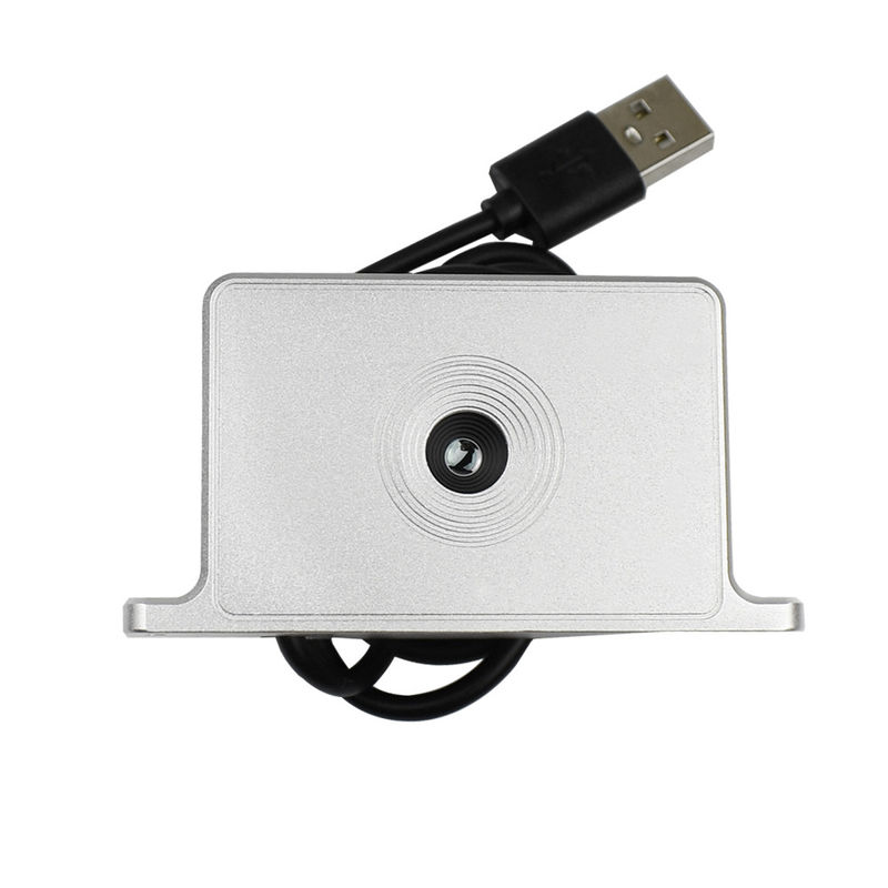
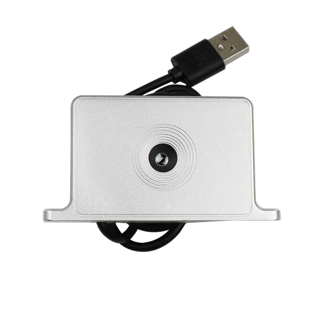
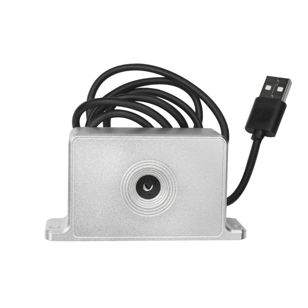
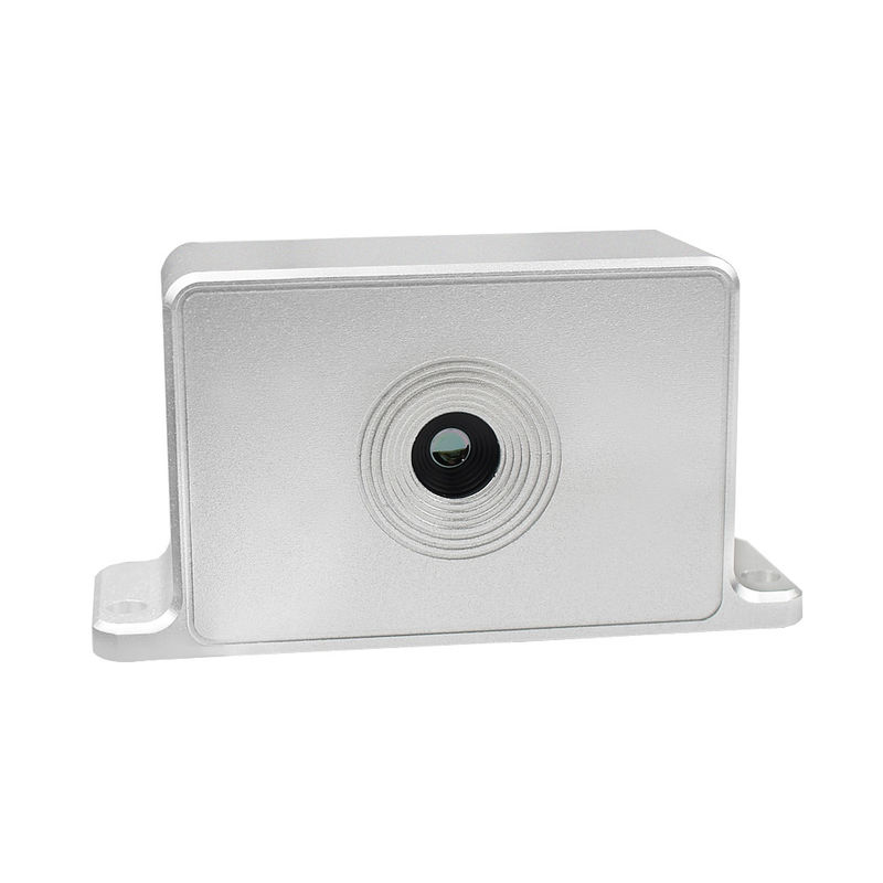
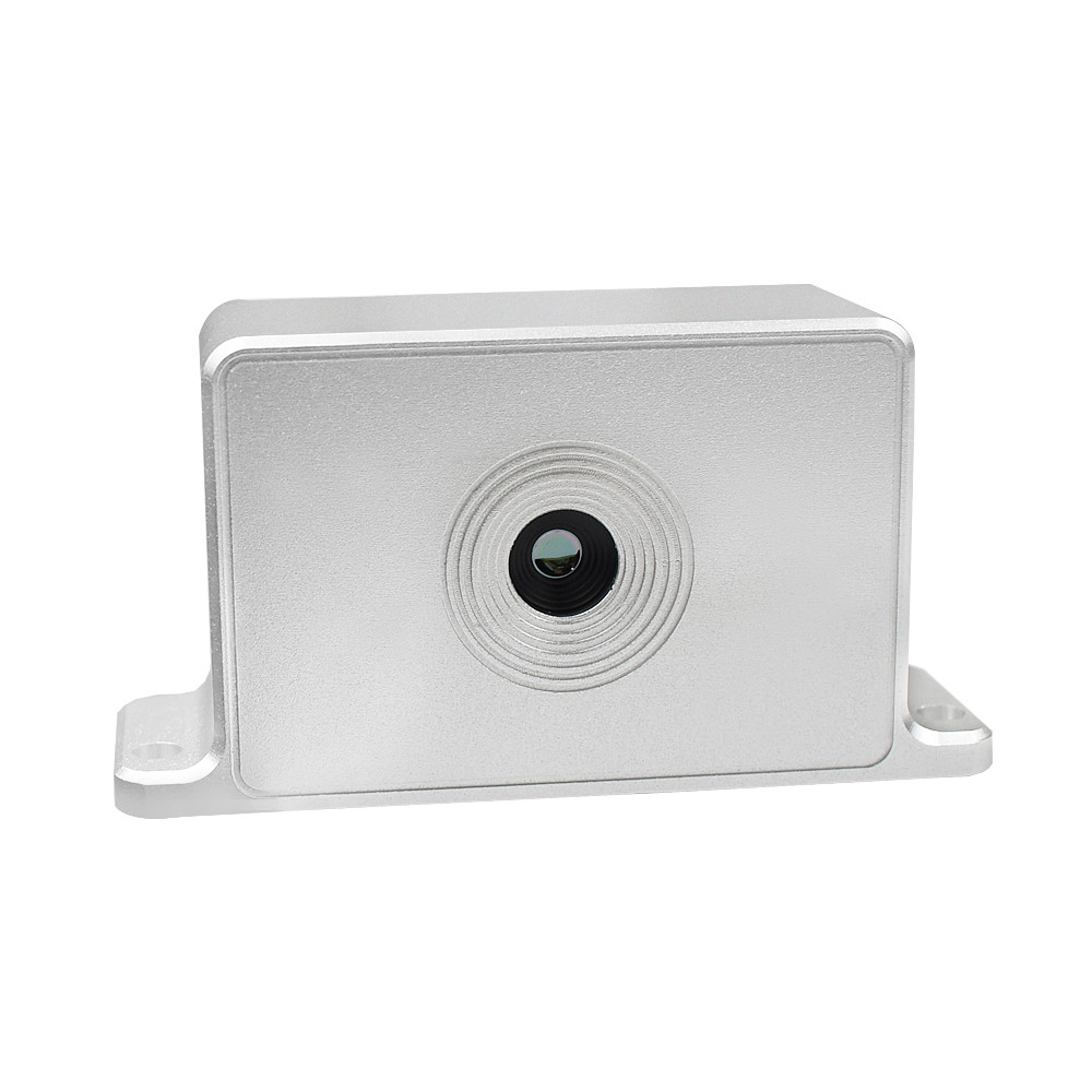
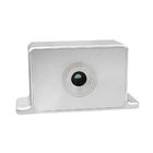
| Name: | Face Recognition Device | Size: | 62mm (L)*42mm(W)*25mm(H); |
|---|---|---|---|
| Resolution: | 256×192 | Cellspacing: | 12μm |
| Angle Of View: | 25.5°×19.2° | Image Frame Rate: | 25Hz/15Hz |
| Highlight: | handheld uhf rfid reader,biometric attendance system face recognition |
||
Scanmax Face Temperature Measurement Module FT10 Datasheet-EN
Face Recognition Device Description
The temperature measuring thermal imaging module is developed based on wafer chip scale packaging uncooled vanadium oxide infrared detector, fit for working with various intelligent platform. It boasts the features of high performance, low power consumption, small size and easy for development and integration. It meets the secondary development requirement of various infrared temperature measuring applications.
Face Recognition Device Features
Small size, easy integrated,size :62mm (L)*42mm(W)*25mm(H);
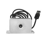
USB interface, easy to connect;
Low power consumption;
High image quality
Accurate temperature measurement;
Standard data interface, supporting secondary development, easy to integrate, and supporting access to various intelligent processing platforms.
Face Recognition Device performance parameters
| Model | FT10 |
| Resolution | 256×192 |
| Cellspacing | 12μm |
| Angle of view | 25.5°×19.2° |
| Image frame rate | 25Hz/15Hz |
| NETD | ≤60mK@f#1.0 |
| Operating temperature | -15℃~+60℃ |
| Supply voltage | 3.8V-5.5V DC |
| Power consumption | <200mW* |
| Weight | <18g |
| Size / mm | 62*42*25 |
| Data interface | Control interface/USB |
| Control interface | SPI/I2C/USB |
| Image enhancement | Multi-gear detail enhancement |
| Picture correction | Shutter correction |
| Swatches | White Hot/Black Hot/Multiple Pseudo Color Options |
| Temp measurement range | 0 ℃ ~ + 60 ℃ |
| Temp measurement accuracy | ± 0.5 ℃ / ± 5% of range |
| Temp correction | Manual / Auto |
| Temperature data output | Real-time parallel output |
| Temp measurement statistics | Support maximum / minimum statistics, Temperature analysis |
| Model | FT10 |
| Resolution | 256×192 |
| Cellspacing | 12μm |
| Angle of view | 25.5°×19.2° |
| Image frame rate | 25Hz/15Hz |
| NETD | ≤60mK@f#1.0 |
| Operating temperature | -15℃~+60℃ |
| Supply voltage | 3.8V-5.5V DC |
| Power consumption | <200mW* |
| weight | <18g |
| Size / mm | 20*20*21 |
| Data interface | Control interface/USB |
| Control interface | SPI/I2C/USB |
| Image enhancement | Multi-gear detail enhancement |
| Picture correction | Shutter correction |
| Swatches | White Hot/Black Hot/Multiple Pseudo Color Options |
| Temp measurement range | -20 ℃ ~ + 120 ℃ (expandable to 600 ℃) |
| Temp measurement accuracy | ± 0.5 ℃ / ± 5% of range |
| Temp correction | Manual / Auto |
| Temperature data output | Real-time parallel output |
| Temp measurement statistics | Support maximum / minimum statistics, Temperature analysis |
* Parallel interface in 25Hz output mode
4 User interface description
The product uses a sub interface, the input voltage is: 3.8 ~ 5.5VDC, does not support overvoltage and undervoltage protection
| Serial No. | Name | Type | Voltage | Description | |
| 1,2 | VCC | Power | -- | Power Supply | |
| 3,4,12 | GND | Power | -- | Ground | |
| 5 | USB_DMj | I/O | -- | USB 2.0 | DM |
| 6 | USB_DPj | I/O | -- | DP | |
| 7 | USBEN*k | I | -- | Enable USB | |
| 8 | SPI_SCK | I | Default:1.8V |
SPI |
SCK |
| 9 | SPI_SDO | O | LVCMOS ; | SDO | |
| 10 | SPI_SDI | I | ( if need 3.3V | SDI | |
| 11 | SPI_SS | I | LVCOMS output, please contact us | SS | |
| 13 | DV_CLK | O | VIDEO | CLK | |
| 14 | DV_VS | O | VS | ||
| 15 | DV_HS | O | HS | ||
| 16 | DV_D0 | O | DATA0 | ||
| 17 | DV_D1 | O | DATA1 | ||
| 18 | DV_D2 | O | DATA2 | ||
| 19 | DV_D3 | O | DATA3 | ||
| 20 | DV_D4 | O | DATA4 | ||
| 21 | DV_D5 | O | DATA5 | ||
| 22 | DV_D6 | O | DATA6 | ||
| 23 | DV_D7 | O | DATA7 | ||
| 24 | DV_D8 | O | DATA8 | ||
| 25 | DV_D9 | O | DATA9 | ||
| 26 | DV_D10 | O | DATA10 | ||
| 27 | DV_D11 | O | DATA11 | ||
| 28 | DV_D12 | O | DATA12 | ||
| 29 | DV_D13 | O | DATA13 | ||
| 30 | DV_D14 | O | DATA14 | ||
| 31 | DV_D15 | O | DATA15 | ||
| 32 | I2C_SCL | I | I2C | SCL | |
| 33 | I2C_SDA | I/O | SDA | ||
Pin5, Pin6 default USB2.0, compatible 3.3V TTL UART interface, if need UART interface pls contact us ; Attention: Pin5: TX; Pin6: RX; TX, RX Relative Xmodule S0;
When the USB_EN pin high level, the 5 and 6 pins working as USB data pins, USB communication uses UVC communication protocol, the image format is YUV422, if you need USB communication development kit, please contact us;
In PCB design, parallel digital video signal 50 Ω impedance suggested.
Table 3 Electrical Characteristics
Typical VIN =4V, TA = 25°C
| Parameter | Symbols | Test Conditions | MIN TYP MAX | Unit |
| Input Voltage Range | VIN | -- | 3.8 4 5.5 | V |
| Load | ILOAD | USBEN=GND | 75 300 | mA |
| USBEN=HIGH | 110 340 | mA | ||
| USB Enable Control | USBEN-LOW | -- | 0.4 | V |
| USBEN- HIGN | -- | 1.4 5.5V | V |
Table 4 Absolute Maximum Ratings
| Parameters | Range |
| VIN to GND | -0.3V to +6V |
| DP,DM to GND | -0.3V to +6V |
| USBEN to GND | -0.3V to 10V |
| SPI to GND | -0.3V to +3.3V |
| VIDEO to GND | -0.3V to +3.3V |
| I2C to GND | -0.3V to +3.3V |
| Storage Temperature | −55°C to +120°C |
| Operating Temperature | −40°C to +85°C |
CAUTION: Meeting or exceeding the ranges listed under Absolute Maximum Ratings may cause permanent damage to the product. Operation that exceeds the maximum working conditions for a long time may affect the reliability of the product.
5. Attention
To protect you and others from injury or protect your device from damage, please read all the information below before using your device.
1. Make sure the camera doesn't look directly at high-intensity radiation sources such as the sun;
2. Do not touch the detector window with your hands or other objects;
3. Do not touch the device and cables with wet hands;
4. Do not bend or damage the connecting cables;
5. Do not scrub your equipment with thinner;
6. Do not plug or unplug other cables without disconnecting power;
7. Please do not connect the attached connecting cable incorrectly to avoid damage to the device;
8. Please pay attention to prevent static electricity;
9. Do not disassemble the device. If there is a malfunction, please contact our company and have it repaired by professionals
Appendix 3 I2C Control Protocol
Table 3 Module I2C address 7bit device address (0x18), read address 0x31, write address 0x30.
| Serial number | Register address | Parameter | Description |
| 1 |
0x80 |
0x00 | Shutter correction * |
| 2 | 0x01 | Background correction | |
| 3 | 0x02 | Detector raw output | |
| 4 | 0x05 | Image data output | |
| 5 | 0x20 | Normal temperature measurement | |
| 6 | 0x21 | Extended temperature measurement | |
| 7 | 0x27 | 16-bit parallel image output | |
| 8 | 0x28 | 8-bit parallel image output | |
| 9 | 0x29 | 16-bit parallel image + temperature data output | |
| 10 | 0x2A | 8-bit parallel image + temperature data output | |
| 11 | 0x2B | Load temperature measurement parameters | |
| 12 | 0xFE | Save configuration parameters | |
| 13 | 0x88 | 0-7 | Swatches |
| 14 | 0x96 | float type | Target reflection temperature (default 25 ℃) |
| 15 | 0x97 | float type | Target ambient temperature (default 25 ℃) |
| 16 | 0x98 | float type | Ambient humidity (default 0.45) |
| 17 | 0x99 | float type | Target emissivity (default 0.98) |
| 18 | 0x9a | float type | Target distance(default 1m) |
* Shutter correction function can correct the non-uniformity of infrared images and the accuracy of temperature measurement; the device needs 5-10min to stabilize during the boot process; the device defaults to 3 times of start-up shutter correction, after that, it is not corrected by default, and the back end can periodically call the shutter correction, correct the image and temperature data.
Register status read:
| Serial Number |
Register address
|
Return parameter
|
Description |
| 1 | 0x01 | 16 bytes | Device PN code |
| 2 | 0x02 | 7 bytes | Device SN code |
| 3 | 0x04 | 16 bytes |
Software version number |
| 4 | 0x05 | 4 bytes | fpa temperature (float type) |
| 5 | 0x06 | 2 bytes | Shutter temperature (same as temperature data format) |
| 6 | 0x0A | 1 byte | Swatches |
|
7 |
0x:80 |
1 byte |
[0-2]: data source [3]: temperature measurement range, 0 normal temperature 1 Wide temperature [4-7]: Parallel interface output type: |
![]()